
Making 1.5-layer PCBs
Even with the dropping prices (down to $10/10pcs) of PCBs manufactured in China, I still find it useful to be able to make your own. Nothing ruins the excitement of a project like waiting 1-2 months for the boards.
I find the alignment of 2-layer boards too cumbersome, and routing 1-layer boards without jumpwires is also difficult. Instead I have found a good compromise that I call 1.5-layer PCBs: only the top layer is etched, while the bottom layer is solid ground plane. This eases routing and improves noise performance while being as easy to make as a 1-layer PCB.
Step 1: Layout
Layout the board normally, and add a polygon fill on the bottom layer (connected to GND signal). You will note that laying out the connections is much easier when ground is available at any point. Pick the via size based on your smallest drill size, no need to worry about alignment.
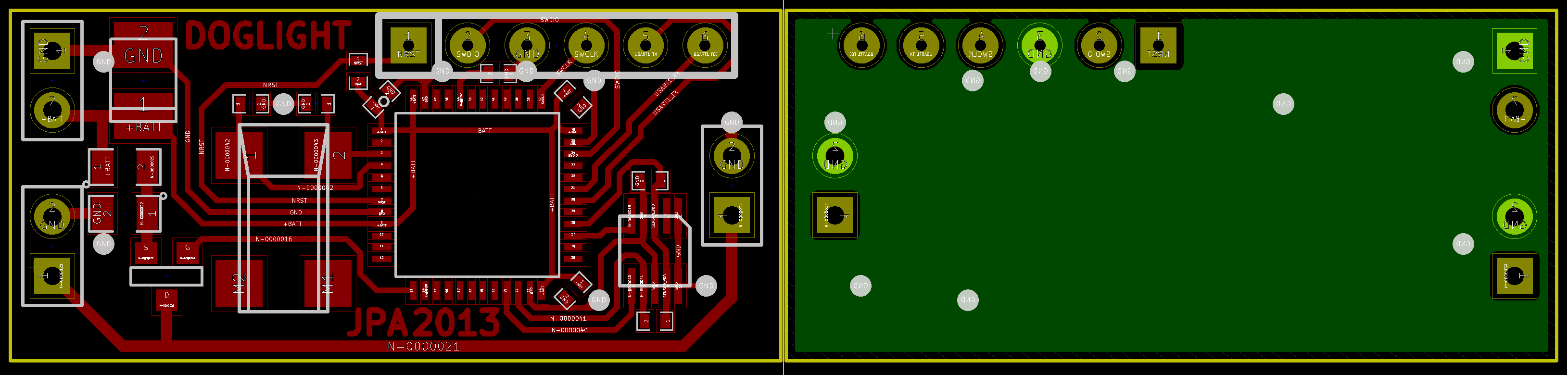 No jumpwires necessary even though there is reasonably many traces.
Step 2: Etching/engraving the PCB
The base material is 2-sided copper-clad board. I'm not going into details on the etching the PCB, as there are plenty of ways to do it. I myself use photoresist and NaSO4 as etchant, but toner transfer, CNC engraving or any other method works just as well with this tutorial. Remember to protect the bottom layer with e.g. tape.
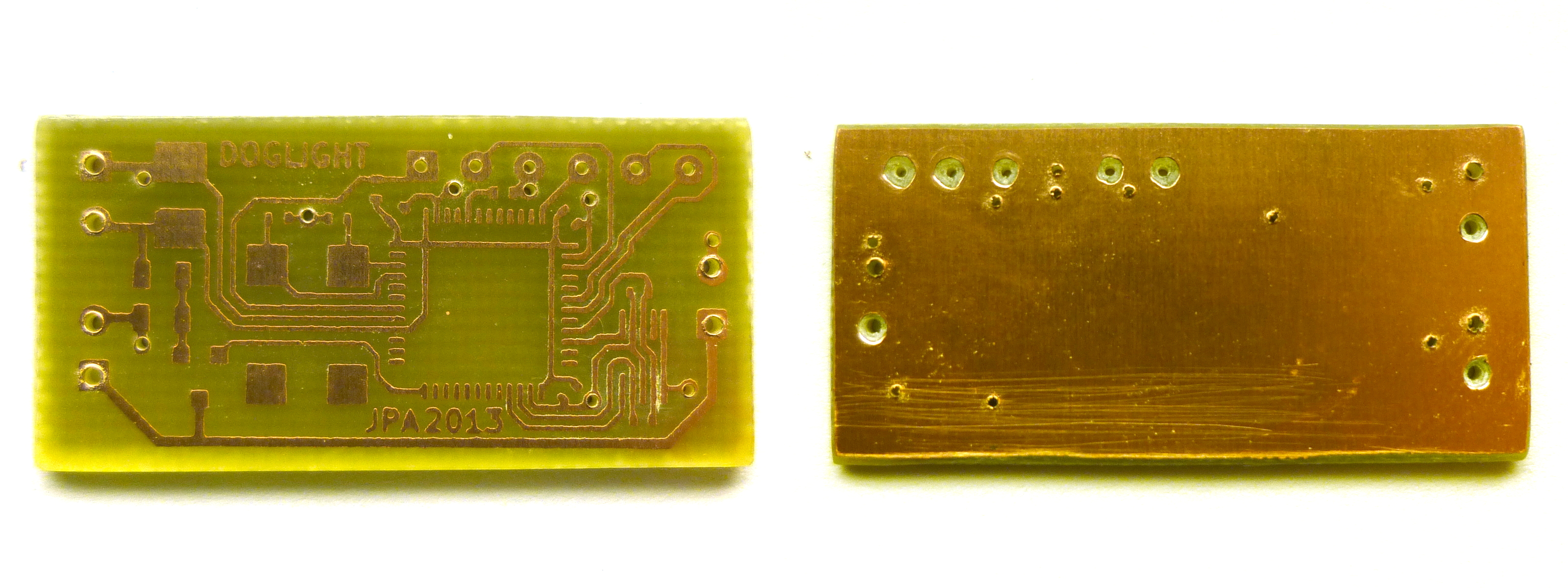
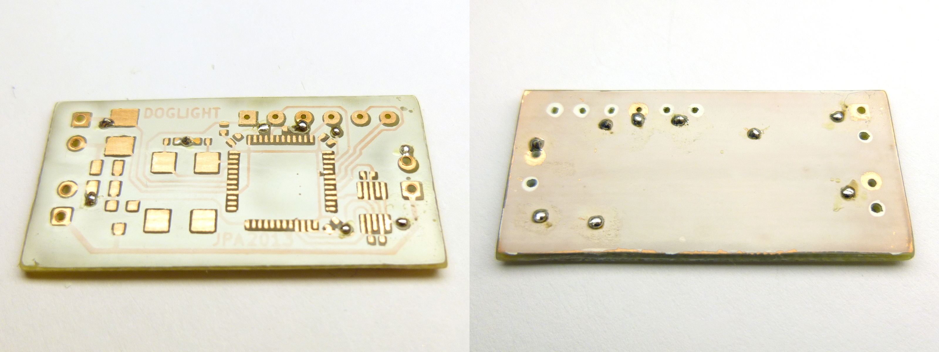
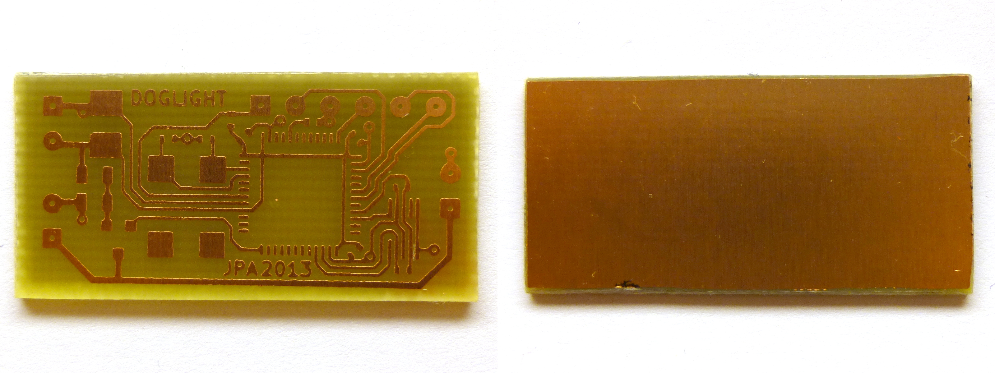 PCB after etching. Only top layer is etched, bottom layer is intact.
Step 3: Drilling the holes
Drill all the holes on the PCB.
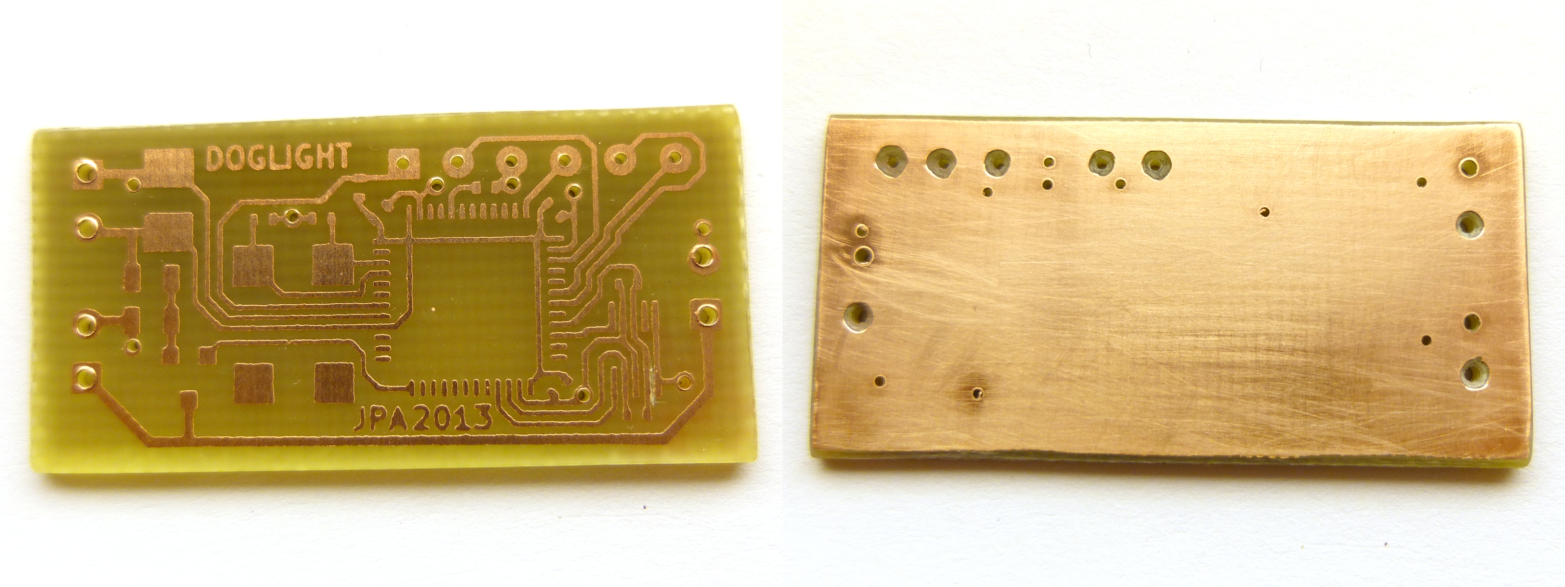
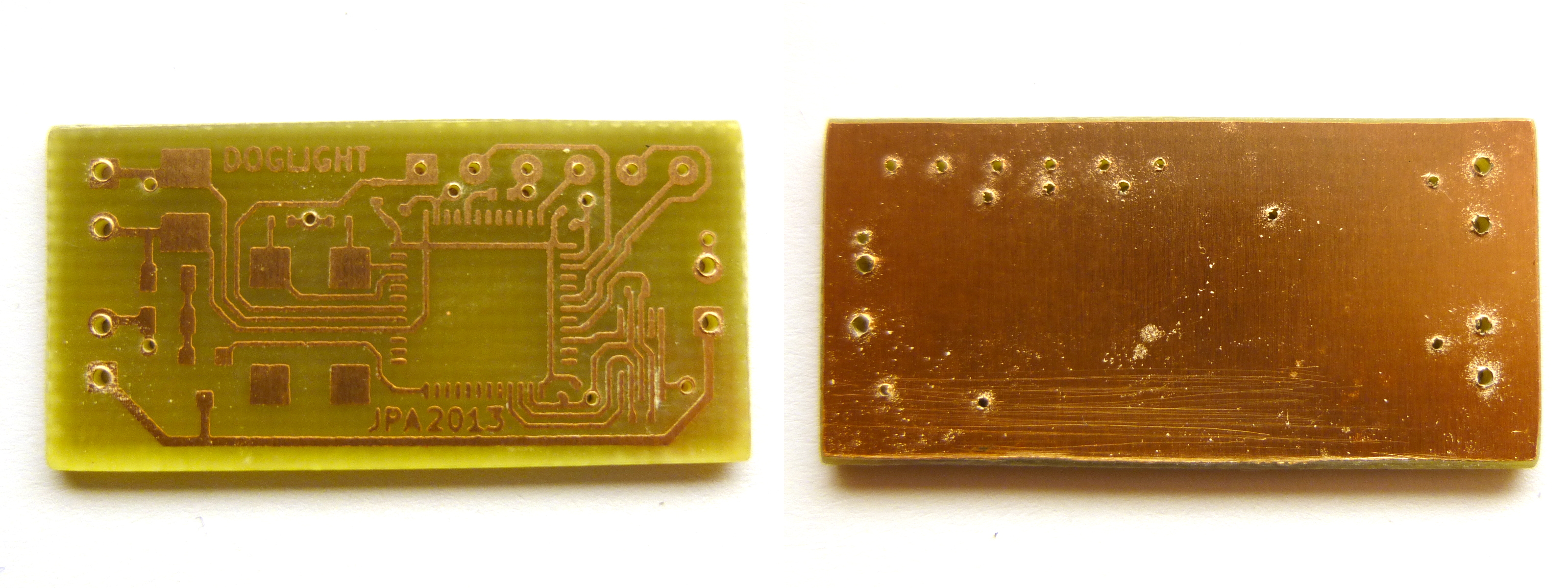 If your drillbits are as dull as mine, you'll get some burrs on the backside copper. Don't worry about it for now.
 My vias are 0.9 mm diameter with 0.5 mm drill. Even with just 0.2 mm ring around the hole there is no problem of alignment, as you can align visually to the top layer.
Step 4: Isolating the holes
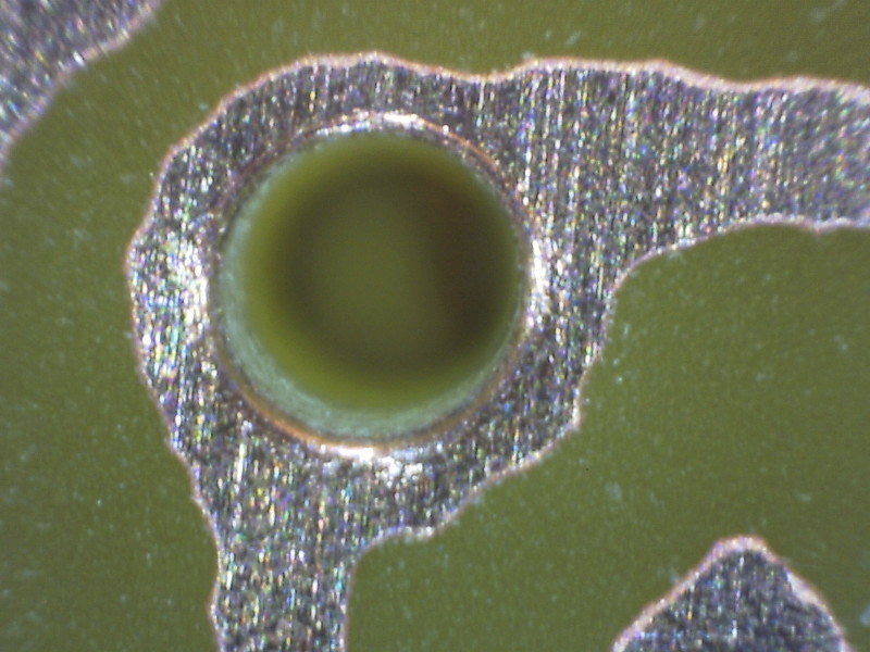
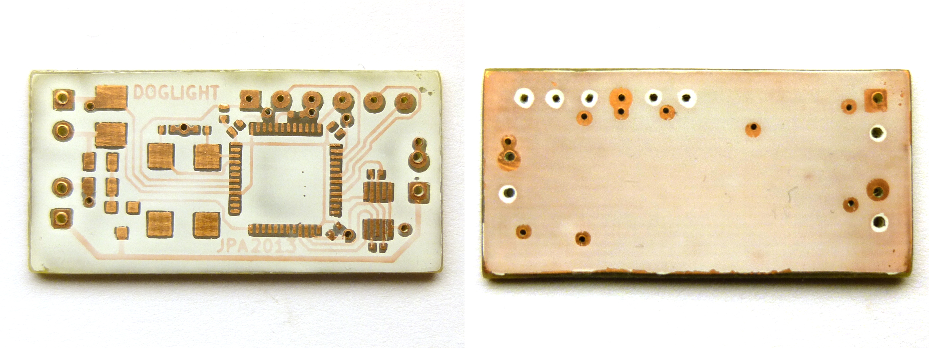
Because the backside is not etched, the copper goes straight against all the holes. The ones that are not actually connected to ground must be isolated. Easiest way to do this is to use a ~4 mm drill bit that you spin by hand in each hole to cut away a bit of copper around it.
 I don't isolate the pins that go into ground anyway, but that is a matter of taste.
Step 5: Deburring
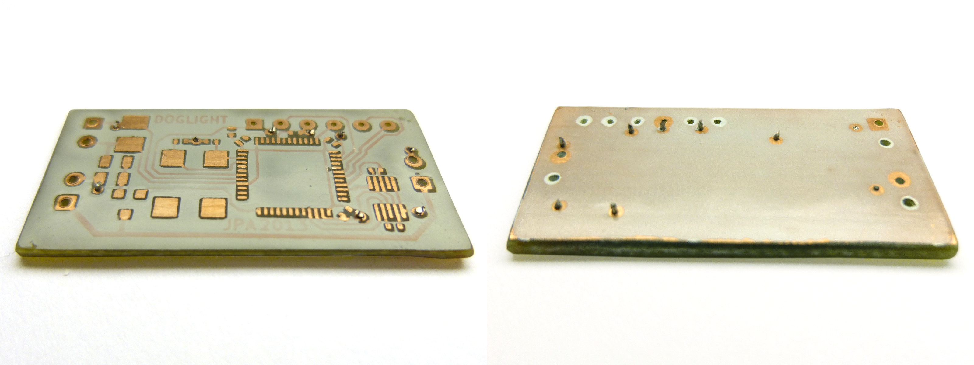
At this point you may or may not have some burrs where the copper has risen up around the hole. If you do, use fine-grit sandpaper (e.g. 1200) to get rid of them.
Step 6: Soldermask (optional)
I have recently begun to do DIY soldermasks using UV curable soldermask paint. This step is totally optional. However, if you do make a soldermask, remember to select do not tent vias because you'll have to solder them.
 It might be easier to get an even coating if you apply the mask before drilling.
Step 7: Soldering the vias
For the vias, you need wire with the same diameter as your via holes. Stick the wire into each hole until it hits the table underneath and then cut it flush with the board.
 It's not all that important how much the wire sticks out of the board; but if it seems to stick too much, just cut it flush again after soldering one side.
I usually stick all the wires in the holes first, and then solder all the vias in one go. You will need to apply considerable heat on the backside for the first few vias until the ground plane heats up.
 Try to get nice round bumps on each via.
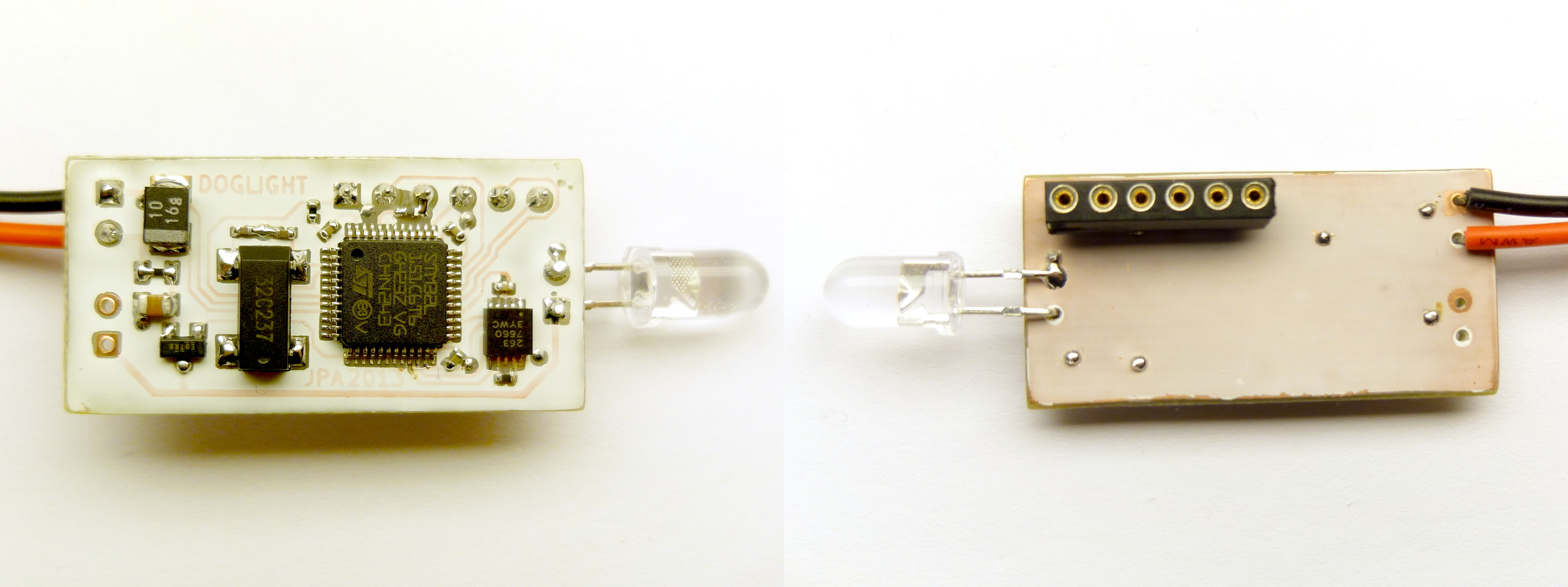
Step 8: Soldering the rest of the components
Now you can go on soldering the rest of the parts. Wash off the flux with alcohol and the board is done.
– Petteri Aimonen on 3.11.2013