TEM cell construction
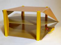
Building a TEM cell is easy in principle: it is just a metal box. But it does require careful dimensioning to work well, and many of the formulas online are just plain wrong.
Impedance matching
The characteristic impedance of a TEM cell is the ratio of voltage and current at each point along its length. Things are simplest if it matches your spectrum analyzer, which typically have 50 ohm inputs. If needed, a transformer or a resistor circuit can adapt between different impedances. Mismatched impedances lead to reflections at connection points, causing attenuation or amplification depending on frequency.
The impedance depends primarily on the ratio between the width of the middle conductor (septum) and the distance to ground planes (shield). Wider septum and smaller distance give lower impedance. The thickness of the material and the width of the shield affect it to a lesser extent, as does anything placed inside the TEM cell. It is usual to aim for an impedance slightly higher than 50 ohms, as a device placed into the cell will reduce the effective distance to ground and thus the impedance.
The quality of matching can be characterized by VSWR measurement. Ideal match would have a VSWR of 1, while a VSWR of 2 means that reflections cause up to 2x difference in amplitude along the cable. In the context of EMC measurements, VSWR of 2 translates to 6 dB uncertainty in the measurement result. The amplitude error caused by impedance matching is frequency dependent, and while it can theoretically be calibrated away, it is easier to just try for a good match.
Even a perfectly matched cell will have resonant frequencies which will limit its usefulness at high frequencies. The first resonance peak will occur at a frequency where the width of the septum fits half a wavelength of signal. The TEM cell can be used even beyond this frequency, but the amplitude response is uneven, increasing the uncertainty of measurements.
Literature research
The history of TEM cells begins with the 1974 article Generation of Standard EM Fields Using TEM Transmission Cells by Myron L. Crawford. It details the basic structure of a TEM cell, its uses and the formula to calculate the impedance. Simplified for air as the material between plates and use of thin material, the impedance is calculated as:
Z0 = 94 ohm / (w / b + Cf / 0.0885)
Where w is the width of the septum and b is the height of the cell. Cf is the fringe capacitance, which Crawford determined experimentally for a few geometries using scale models.
Crawford's results are excellent, achieving VSWR of under 1.2 up to the resonant frequency of the cell. In his case, the septum is 1.2 meters wide, leading to a low resonant frequency of 125 MHz. A smaller cell will have higher resonant frequency, but there is less space to fit devices inside. Fortunately the electronics we have in 2023 are much smaller than the electronics of 1974.
Skip forward to 2008. TEM cells are popular and widely used, but commercially available ones are expensive. Sandeep M. Satav published the paper Do-it-Yourself Fabrication of an Open TEM Cell for EMC Pre-compliance which used PCB material for the construction of an open TEM cell. Very good idea and easy to manufacture, and the construction method has found popularity in the DIY community.
Unfortunately there is a small mistake in the geometry calculations. Satav uses the rectangular geometry described in Crawford's paper, and the value Cf = 0.053 for fringe capacitance that Crawford determined experimentally. But Crawford used closed TEM cells, which have four metal walls. Satav's paper shows an open TEM cell with only two walls - easier to build and use, though less shielded from outside noise. The fringe capacitance 0.053 is an incorrect value for an open TEM cell.
The error in the geometry yields a characteristic impedance of about 70 ohms. While still usable, this shows up as less-than-ideal VSWR of over 2 in Satav's results.
Later in 2020, Michal Hrouda built a cell using Satav's dimensions, yielding similar performance.
Scale models
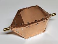
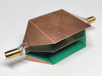
To verify that I was indeed correct about the mistake in dimensions, I decided to follow Crawford's example and built a scale model. For material I used cardboard and copper tape, with a printed template to cut them accurately to size.
For the first prototype, I chose the square cross section from Crawford's paper, scaled down to 40 mm shield width and 33 mm septum width. At first I built it without the side walls. With 50 ohm terminator at the other end, the S11 measurement done with NanoVNA V2 showed wildly varying impedance. This is because the TEM cell acts as a quarter-wave impedance transformer.
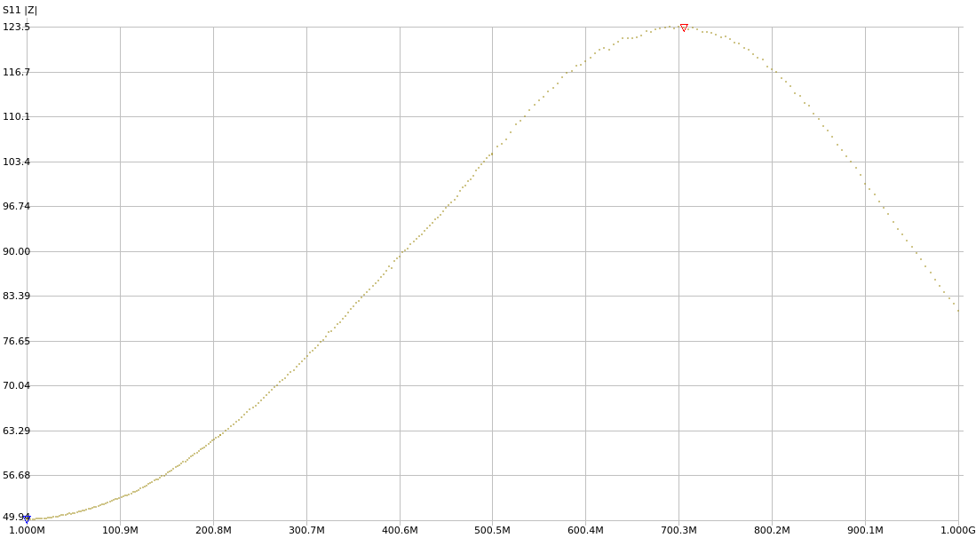
The 700 MHz peak frequency matches a quarter wave with the 100 mm length of the cell. From the 123 ohm peak impedance, we can deduce a characteristic impedance of sqrt(50 ohm * 123 ohm) = 78 ohm. From this, we can calculate the actual fringe capacitance value and find it to be 0.033.
To verify that open vs. closed TEM cell makes a difference for the geometry, I then added side walls and got characteristic impedance of 57 ohms.
Finally, I calculated new dimensions for an open cell with Cf = 0.033, built a scale model and got a characteristic impedance of 55 ohms. I adjusted my final estimate of Cf down to 0.03.
Size of the box
The larger the TEM cell, the bigger devices you can fit into it. The common advice is to occupy at most 1/3rd of the vertical space. And for proper coverage, you'd want to rotate the device into all three major orientations. For 100 mm plate separation, that would give maximum device size of just 30x30x30 mm.
I decided to disregard this, because I don't have the room to store a huge box. 100 mm plate separation would have to do. With the 0.03 value I obtained earlier, I calculated 300 mm as suitable width of the septum. I scaled the shields in same ratio to 350 mm wide.
Another size decision I made was to have the ends taper at an angle of 45 degrees. Shallower angle gives better impedance match in the tapered section, but it also increases the length a lot.
I had already bought some PCB material in three sheets of 610x457 mm. With the 45 degree taper angle, center section length would be 300 mm and each tapered section takes 150 mm of material, for a total of 600 mm. This allowed me to fit each of the three parts on its own sheet, minimizing cutting and joining of the pieces.
Cutting the sheets
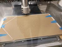
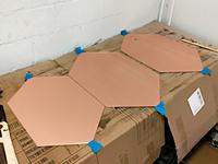
For me, CNC router was the obvious choice for cutting the PCB sheets. But this could equally well be done with a jigsaw or just about any saw - a few millimeters of inaccuracy doesn't make much difference.
The material I used was 1-sided PCB sheet from TME. Solid sheet of copper, brass or aluminum would work equally well electrically. I have seen other projects use double-sided PCB and joining the sides by soldering wires through holes, but I don't think that is necessary for the power levels involved.
Construction


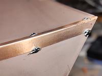
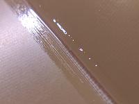
The shield pieces on top and bottom have a bend to them - 45 degrees in my design, 30 degrees in designs with a shallower taper. My plan was to route a slot almost all the way through the PCB material, to bend the sheet and use epoxy glue to fix the angle. This would avoid having to solder together multiple pieces and ensure a continuous copper surface.
Unfortunately the copper layer disagreed with me and ripped apart in multiple places. To fix this I used copper tape and soldered bridges every few centimeters. Another layer of copper tape on top, and it should bridge the pieces well enough.
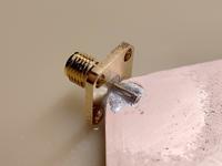
I chose to use SMA connectors at each end. My initial plan was to just solder the septum to the middle pin and the shields to the body of the connector. I quickly found out that this put way too much load on the connector middle pin, and resorted to using epoxy to keep the septum in place.
In the center section the correct distance and alignment of the sheets is maintained by 3D printed side supports. I printed these at lowest infill setting to reduce their effect on capacitance.
In retrospect the best orientation would be to have insulating sides of each PCB towards the device being tested. This avoids any accidental contact to the conductive surfaces. I happened to solder the septum the opposite way around, but I can always add a plastic film for insulation.
Results
I used NanoVNA V2 to measure the cell parameters. I collected the previosuly published measurement results for comparison:
- Generation of Standard EM Fields Using TEM Transmission Cells by Myron L. Crawford et al, 1974. Closed 4-wall 1.5 meter wide TEM cell made of 3 mm aluminum sheet.
- Do-it-Yourself Fabrication of an Open TEM Cell for EMC Pre-compliance by Sandeep M. Satav et al, 2008. Open 30 cm wide TEM cell made of double-sided FR4 PCB material.
- Tekbox TBTC2, first released in 2016. Open 30 cm wide TEM cell, shields made of solid aluminum and septum from PCB material. Special construction of septum reduces high-frequency resonances.
- Making TEM cell for EMC measurements by Michal Hrouda, 2020. Open 30 cm wide TEM cell made of 0.5 mm copper sheet.
- Increasing the Test-Volume of Open TEM Cells by Using an Asymmetric Design, by Christian Spindelberger et al, 2022. Asymmetric open 30 cm wide TEM cell made of 3 mm aluminum sheet.
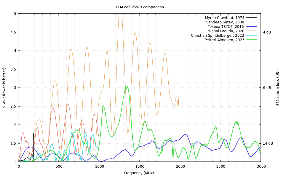
The results appear to confirm that the dimensions presented in 2. and used also in 4. are suboptimal. Tekbox TBTC2 is superior in high-frequency performance. In frequencies less than 500 MHz all correctly dimensioned cells give VSWR under 1.5, which is perfectly fine for all EMC pretesting purposes.
Further improvements
Christian Spindelberger's paper details an asymmetric TEM cell design, which has a higher lower section and thin upper section. This makes much better use of vertical space, as in a symmetric cell the upper partition doesn't have any practical use. I'm not entirely sure how the asymmetry would affect the sensitivity of measurements.
Tekbox uses slots in the septum copper, bridged by some kind of ferrite or resistive material. This dampens any perpendicular electromagnetic fields and reduces high frequency resonances. A similar technique is explained in "Expanding the Bandwidth of TEM Cells for EMC Measurements" by Myron L. Crawford, 1978 (DOI: 10.1109/TEMC.1978.303664), but instead of slotting the copper it uses absorbent material near the shield. Again I do not know if these methods will effect sensitivity of the measurements.
Design files
I have made a parametric FreeCAD design of the TEM cell I constructed. The main dimensions are in a spreadsheet element and can be adjusted to custom dimensions. The 3D model dimensions will then automatically update to match.
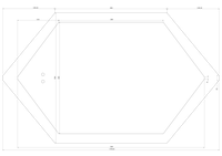
The design files are available GitHub and the basic dimensions also in PDF files linked below:

– Petteri Aimonen on 31.10.2023
