Integrated LISN

Measurement of conducted emissions is as simple as measuring either the voltage or current at the cables going to the device. Typically this is done for the power cables. Most common way is to measure voltage when power is supplied through a line impedance stabilization network.
The purpose of a LISN is to present a consistent 50 ohm impedance towards the device. Any noise currents then yield a predictable noise voltage that can be measured.
For very low power devices, a simple series resistor could be used. But most devices draw too much power to be supplied through a 50 ohm resistor, so an inductor is used instead. Common types are 5 µH and 50 µH LISNs, depending on the lowest frequency being measured. For pretesting, a 50 µH LISN can be used for all standards, as it covers the widest frequency range. Most LISNs also include a prefilter to eliminate any noise conducted from the DC power supply towards the device.
Traditionally LISN and TEM cells are entirely separate pieces of equipment. I chose to integrate a LISN directly to my TEM cell. This makes things simpler in several ways:
- Supplying power through the LISN prevents external noise from affecting radiated emissions measurements.
- Conducted emissions measurements are performed on top of a ground plate, and the TEM cell already has a ground plate.
- Being able to quickly compare radiated and conducted emissions gives clues to where the noise originates from.
Design
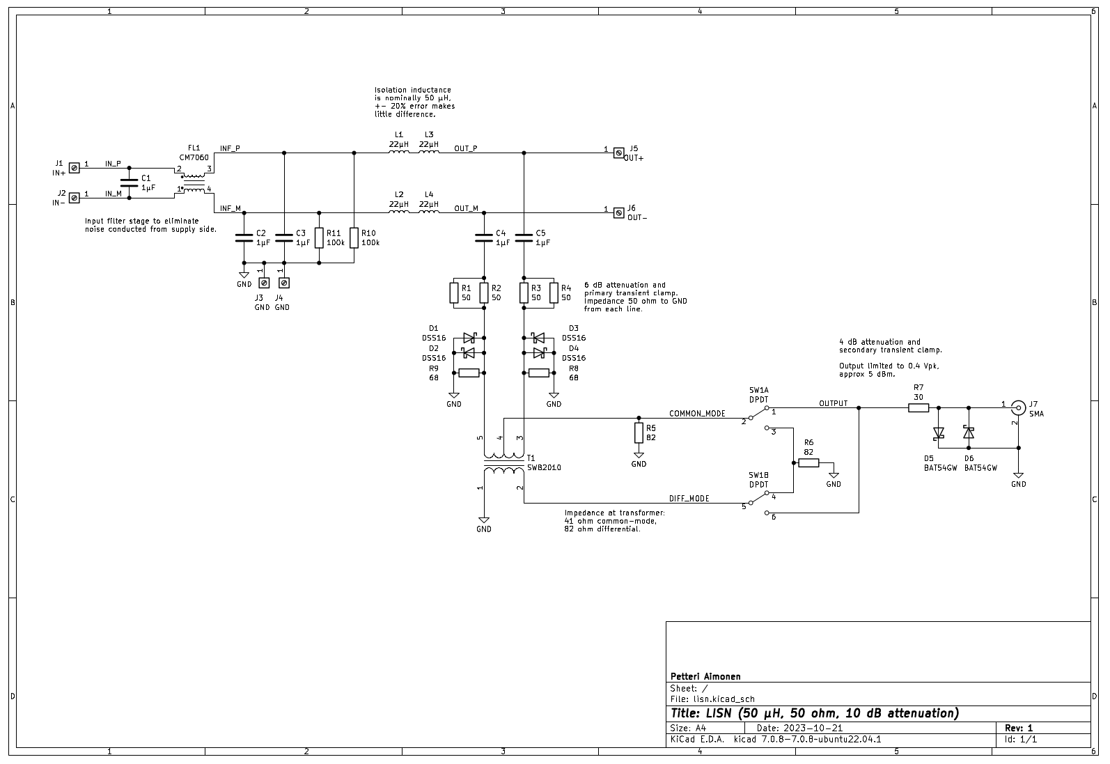
I followed the basic design of LISN described in CISPR-16. A two wire LISN has two output ports. Depending on model they are connected either directly to the positive and negative terminal, or through a transformer to separate the common mode and differential mode noise. First type is simpler, but requires extra math on the measurement instrument. For easy use, I decided to include a transformer.

The input section consists of capacitors and a common mode choke. Their purpose is to block any noise coming from the power supply. Next are the series inductors. I used 2x 22µH on each line, for total of 44 µH. This is close enough to 50 µH for my purposes. A single inductor is fine too, but make sure to stay well below the saturation current rating of the components.
The output of the inductors goes straight to the connectors for the device being tested. The output is also connected through capacitors to the measurement instrument. In the simplest form, each capacitor would go to a coaxial connector, to which the 50 ohm impedance measurement instrument would be connected. At high frequencies, the series inductors have high impedance, while the capacitors act as shorts. For example, at 1 MHz a 50 µH inductor has 314 ohm impedance and 1 µF capacitor has 0.1 ohms. This arrangement directly presents the measurement instrument's 50 ohm impedance to the load.
But instead of measuring each wire separately, we want to know if they fluctuate together (common mode) or inversely (differential mode). A transformer can be used to calculate both the average and the difference between the channels.
Finally, there is a need to protect the measurement instrument from sudden transitions. For tinySA Ultra, the maximum input level is 6 dBm or about 0.5 volts. Turning on a 12 volt supply would result in a spike far higher than this, as would any accidental short-circuit or disconnection. Some voltage clamping is needed, and this will result in a bit of signal attenuation. I aimed for 10 dB attenuation in order to not decrease the sensitivity too much.
I did the output clamping in two stages. First stage consists of 25 ohm series resistance and four high-current DSS16 schottky diodes. These will clamp even large transients to 1 volt peak voltage on each line, while giving 6 dB of attenuation.
This is followed by the differential/common mode transformer setup. I selected SWB2010 RF transformer because it has the middle tap needed for common mode measurement. The models SWB1010 and SWB3010 are equally suitable, only difference is that the middle pin is cut shorter. A double-pole switch connects either the transformer secondary or the middle tap of the primary to the output circuit.
From the transformer the signal goes through 30 ohm resistance to a pair of BAT54 diodes that form the second clamp. These do not tolerate large current spikes, but act faster and with smaller dropout voltage. Because there is only about a volt coming into this stage, the current that passes through the 30 ohm resistor is less than 50 mA.
Despite these series resistors, the impedance at the capacitors should be kept at 50 ohms. This is accomplished by a few dummy load resistors connected between the signals and ground. These will dissipate as heat 90% of the input signal, leaving the 10% for the 10dB attenuated output connector. As an extra benefit, the LISN will now have a reasonably correct impedance even when no measurement instrument is connected.
Circuit board and enclosure

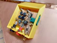
The PCB is a single-layer design, suitable for home etching or CNC routing. SMD parts are used, but nothing excessively tiny. The resistors are of 0603 type because that is what I commonly use, but 0805 would fit too.
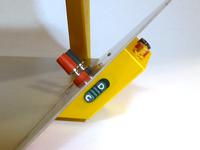
I designed the circuit to be mounted to the TEM cell wall, with binding posts going to the device and banana jack connectors towards the power supply. A pair of M3 mounting holes provide the ground connection to the TEM cell shield through metal standoffs that I soldered to the copper.
The enclosure is 3D printed. It has a slider knob on the side that will hook into the switch on the PCB. By using shorter metal standoffs to attach the PCB, the same holes can also be used for mounting screws to hold down the lid.
Results
An ideal LISN would present 50 ohm impedance from each output terminal to ground at all measurement frequencies. In practice this is not feasible, so test standards specify either 5 µH or 50 µH series inductance to be used. For a 50 µH LISN, measurement range is usually 9 kHz to 100 MHz.
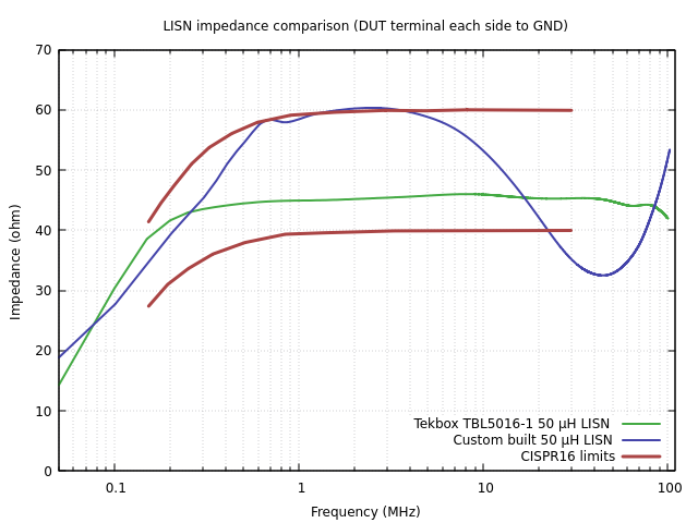
I measured the impedance using NanoVNA V2 and made a comparison against Tekbox TBL5016-1.

The impedance on my build fluctuates quite a bit, but almost remains within the limits set by CISPR16 standard. I'm not sure what causes higher than expected impedance at the middle frequencies. The drop at high frequencies could be due to PCB stray capacitance.
Design files
KiCad design files are available on GitHub.
– Petteri Aimonen on 31.10.2023
