
Logic analyzer application

This logic analyzer application is my second custom program for the DSO Quad. The device has buffer space for 4096 samples by default, which is enough for analog work but somewhat limiting with digital signals. Furthermore, the default firmware makes browsing cumbersome by not letting you change the timebase when the capture is paused.
This program only stores the transitions: if there is no traffic on the wires, no buffer space is consumed. About 20 kB of RAM is allocated for the buffer, which equals 10 to 20 thousand events. For example, this is plenty for 2 kB of data traffic on an RS232 line.
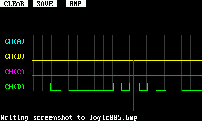
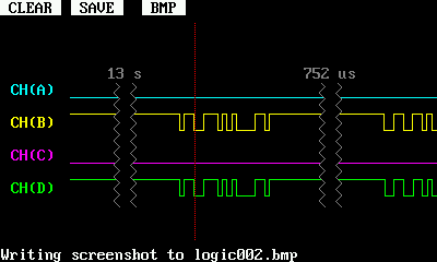 Long idle periods are collapsed on screen.
I have tried to make navigating the signal as easy as possible. The two navigation switches are dedicated to zooming and scrolling, and both of these work quite fast. Only at the smallest zoom levels the scrolling will slow down, as redrawing the whole signal takes time. I intend to improve the performance in the future by adding some caching of the intermediate values.
Signal capture
The default FPGA logic has an interesting interpretation of a FIFO. It allows you to read through it once (4096 samples), but after that you have to reset it to get any new data. I guess that makes sense when using it only as an oscilloscope, but it makes real-time analysis of the data a pain.
Fortunately, it has a quirk that overwrites the last value if you keep reading past the end of the buffer. This allows kind of bypassing the FPGA, and reading the raw data as it comes in. There is still a small complication: the results contain 18 bits, which must be read in two parts through the 16-bit bus. The multiplexing is controlled by a signal called H_L (for high/low? heh :) which is connected to GPIOC5 on the STM32 processor (schematics). This in turn is a pin with no super-powers, i.e. no timer output and no FSMC control signals. So, do we need to spend all time in software polling the inputs?
Turns out that no. The DMA controller on the STM32 is very flexible. I arranged it so that one DMA channel constantly writes 0's and 1's to the GPIOC5, while another channel reads the input data into memory between the writes. Once in a while an interrupt routine goes through the DMA memory buffer and checks for any transitions. The transitions are then encoded using length + levels notation, and stored to a larger buffer.
This method gives a sample rate of 500 kHz, which is enough for low-speed RS232, I2C etc. debugging. The nice thing is that the capture can run all the time, and you can watch the signal as it updates.
Unfortunately I don't have a license for Silicon Blue iCEcube2, so I cannot update the FPGA circuit. The FPGA development environment is free now that Lattice bought SiliconBlueTech. When I get the bitfile loading working, I can implement the logic capture in hardware. That would easily encode all 4 channels at 72MHz.
Display drawing
 The grid automatically adjusts to the signals.
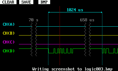 Time measurements, accessed by clicking the scroller.
Merely capturing the signal is not enough, of course. The easiest way to draw it to the screen is to call BIOS routines like __Display_Str and __LCD_SetPixl. These routines, however, draw the graphics pixel-by-pixel. Writing individual pixels all the way to the screen is slow.
The 200 kB framebuffer won't fit in the 48 kB RAM of the processor either. So we are left with the method partially used in the original firmware: rendering the graphics line by line, and transferring them to the screen at the same time. The original firmware only uses this for the oscilloscope graphs, but I implemented a few simple classes, such as TextDrawable, so that I can avoid the pixel-by-pixel operations completely.
The result is very fast screen update - it typically takes only 10 milliseconds. This makes scrolling a pleasure, atleast until a few bottlenecks elsewhere in my code start to limit the speed with large signals.
Installation and use
Note: There are some deficiencies in the channels C & D input protection stage which may limit the maximum safe voltage. However, further analysis suggests that the issue is not that bad. Voltages up to 5V are almost certainly safe and probably even voltages up to 20V. Just thought you should know. Channels A and B should handle larger voltages, up to 80 volts.
You can download the program from here.
The HEX-file installs as the application 3, so you have to hold the third button when turning on the DSO Quad. Otherwise the installation is the same as for the frequency response application.
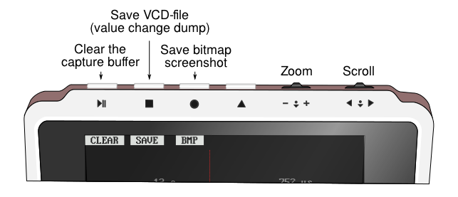
The three buttons on the left allow restarting the capture, and saving either all the data as a VCD file or the currently visible part as a .BMP screenshot. The VCD format can be read by many wave viewers on the PC, such as GTKWave.
The source code is available on GitHub.
– Petteri Aimonen on 12.1.2012