
BGA inspection using plastic prisms
BGA (Ball Grid Array) packaging for microchips is getting more common as devices become smaller. It's quite feasible to solder with a basic home reflow setup, but verifying the results is difficult. The gold standard would be X-ray imaging, but short of that you can use optical verification with simple prism tools.
Optical verification principle
The idea is to shine light from the side, so that it passes between the ball rows beneath the chip. This will indicate any short-circuits between the rows, but will not show any missing balls. It will, however, show insufficiently melted solder paste or uneven distribution of solder. So if the chip began with all balls present and the solder paste was applied evenly on the PCB, you can be reasonably confident that any faults would be visible.

If there were no other components on the PCB, you could simply hold the PCB edgewise against a bright background and observe from the side. You would then see the balls as dark shadows against the background.
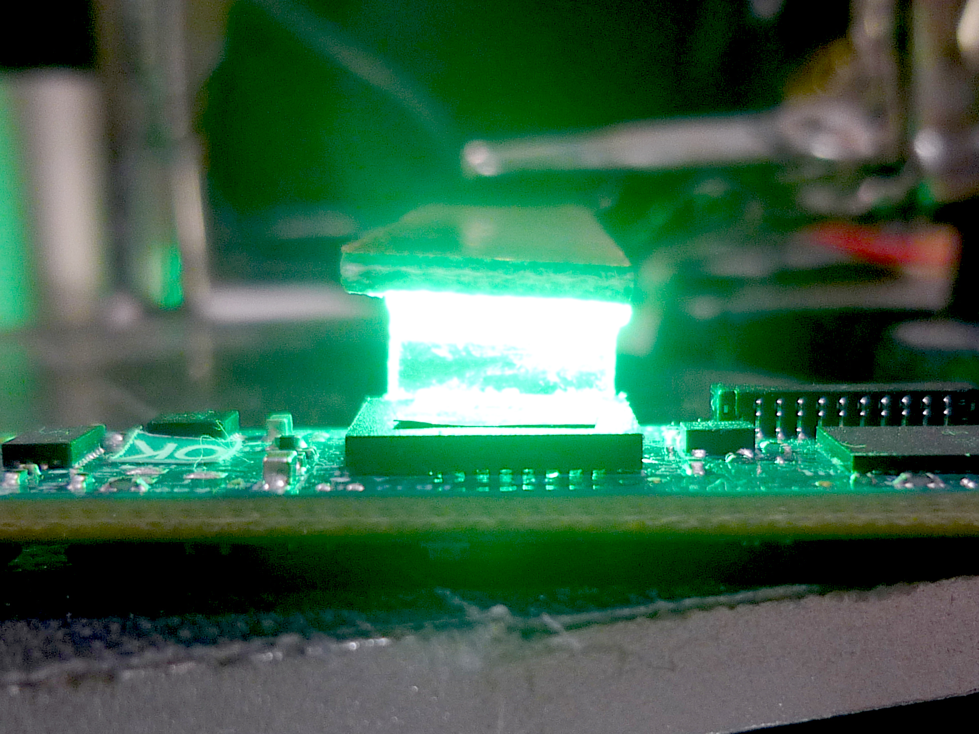
However, practical PCBs don't have much space around the BGA chips so this is rarely possible. Instead, we can use a thin prism to redirect light in 90° angle around the corner of the chip. By cutting and polishing 45° angle in a transparent piece of plastic, total internal reflection makes it act like a mirror. The light from a LED will be directed under the chip, and any light that gets through is mirrored upwards towards the viewer.

Making the prisms


I made my first prototypes from 2 mm thick acrylic. But then I found out that many PCBs leave only about 1 millimeter of space around BGA chips. I didn't have any flat sheets of plastic that thin, but searching through my shelves I figured that Gillette shaving blade cartridges are made of thin transparent plastic.
I cut the pieces into small rectangles and used increasing grids of sandpaper to form the edge and polish it. After 1200 grit, I used 1 micron polishing paste and then Displex plastic polishing paste. This gave a reasonably clean edge, though with some guides I could have gotten it more straight and flat.
Light source


The light source needs to be very bright to be visible though the two prisms. It helps use colored LEDs, which are more easily seen against other ambient lighting.
I used 11 pcs of 0603 high-intensity green LEDs, soldered in parallel side to side. Resistors are used to limit the current to 20 mA per LED.
The prism is superglued onto the LEDs. Superglue has similar refractive index as most plastics, so it reduces losses in the optical interface. It is a good idea to let the glue cure in front of a fan, as otherwise superglue vapours can fog up the prism surfaces.
Results


The prisms work reasonably well. I could probably make them a bit more accurate, and if I made them out of optical quality glass the reflection would probably be clearer.
Even with these quickly made prisms it is easy to see the balls of a 0.5 mm pitch BGA chip. The prism surfaces are not perfectly flat because I held it by hand while polishing. This causes some distortion and extra reflections in the result image.
The biggest drawback of optical inspection is the sensitivity to any flux residue underneath the chip. I have found that freshly reflow-soldered chips are fairly clean underneath after a bit of rinsing with isopropyl alcohol. But when reworking BGA chips it is common to apply an excess of flux, which tends to harden after cooling. Even though it is soluble in isopropanol, cleaning it away takes a lot of effort as it is difficult to get liquid flowing underneath the chip and any brushes won't fit.
– Petteri Aimonen on 26.4.2024